
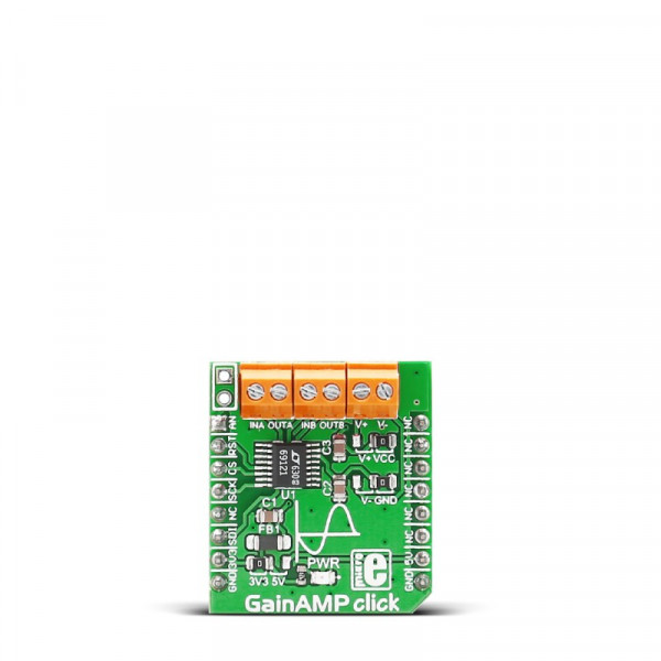
GainAMP click


- Order number: MIKROE-2555
- Manufacturer product ID: MIKROE-2555
GainAMP click carries the LTC®6912 dual channel, low noise, digitally programmable gain amplifier (PGA). The click is designed to work on either 3.3V or 5V power supply. It communicates with the target MCU over SPI interface, with additional functionality provided by the following pins on the mikroBUS™ line: AN, RST.
GainAMP click also features three pairs of screw terminals and a power indication LED.
How it works
The gains for both channels are independently programmable, using a 3-wire SPI interface to select voltage gains of 0, 1, 2, 5, 10, 20, 50, and 100V/V(LTC6912-1). All gains are inverting.
The LTC®6912 consists of 2 matched amplifiers with rail-to-rail outputs. When operated with unity gain, they will also process rail-to-rail input signals.
A half-supply reference generated internally at the AGND pin supports single power supply applications. Operating from single or split supplies from 2.7V to 10.5V total.
Programmable gain amplifier
A programmable-gain amplifier (PGA) is an electronic amplifier whose gain can be controlled externally (by analog or digital signals).
Specifications
| Type | Amplifier |
| Applications | Data Acquisition Systems, Dynamic Gain Changing, Automatic Ranging Circuits, Automatic Gain Control. |
| MCU | LTC®6912 dual channel gain amplifier |
| Key Features | Rail-to-Rail Output Swing, Rail-to-Rail Input Range, 2 Channels with Independent Gain Control, Three pairs of screw terminals, 3-wire SPI interface |
| Interface | SPI,Analog,GPIO |
| Input Voltage | 3.3V or 5V |
| Compatibility | mikroBUS |
| Click board size | S (28.6 x 25.4 mm) |
Pinout diagram
This table shows how the pinout on GainAMP click corresponds to the pinout on the mikroBUS™ socket (the latter shown in the two middle columns).
| Notes | Pin | Pin | Notes | ||||
|---|---|---|---|---|---|---|---|
| Analog input | AN_IN | 1 | AN | PWM | 16 | NC | |
| Shut down | SHDN | 2 | RST | INT | 15 | NC | |
| Chip select | SPI_CS | 3 | CS | TX | 14 | NC | |
| SPI Clock Input | SPI_CLK | 4 | SCK | RX | 13 | NC | |
| NC | 5 | MISO | SCL | 12 | NC | ||
| SPI Master Output Slave Input | SPI_MOSI | 6 | MOSI | SDA | 11 | NC | |
| Power supply | +3.3V | 7 | 3.3V | 5V | 10 | +5V | Power supply |
| Ground | GND | 8 | GND | GND | 9 | GND | Ground |
Maximum ratings
| Description | Min | Typ | Max | Unit |
|---|---|---|---|---|
| Total Supply Voltage (V+ to V–) | 11V | V | ||
| Input Current | ±10 | mA | ||
| Operating Temperature Range | –40°C | 85°C |
Jumpers and settings
| Designator | Name | Default Position | Default Option | Description |
|---|---|---|---|---|
| JP1 | AN_sel | ON | AN | Analog input jumper. |
| JP2 | V+ | Left | VCC | V+ selection. |
| JP3 | V- | Left | GND | V- selection. |
Programming
Code examples for GainAMP click, written for MikroElektronika hardware and compilers are available on Libstock.
The gains for both channels are independently programmable using an SPI interface to select voltage gains. The example controls channel A, increasing and decreasing gain with input buttons.
Code snippet
The code snippet demonstrates a simple usage of the helper function.
01 void main()
02 {
03     system_init();
04
05     gain_amp_set(GAIN_AMP_NOMINAL_0, GAIN_AMP_SW_SHUTDOWN);
06
07     while( 1 )
08     {
09         if(Button(&GPIOE_IDR, 9, 100, 1))
10         {
11             byte = gain_amp_set(++gain & 0x07, GAIN_AMP_SW_SHUTDOWN);
12             GPIOD_ODR = (GPIOD_ODR & 0xFF00) | byte;
13         }
14         if(Button(&GPIOE_IDR, 8, 100, 1))
15         {
16             byte = gain_amp_set(--gain & 0x07, GAIN_AMP_SW_SHUTDOWN);
17             GPIOD_ODR = (GPIOD_ODR & 0xFF00) | byte;
18         }
19     }
20 }