
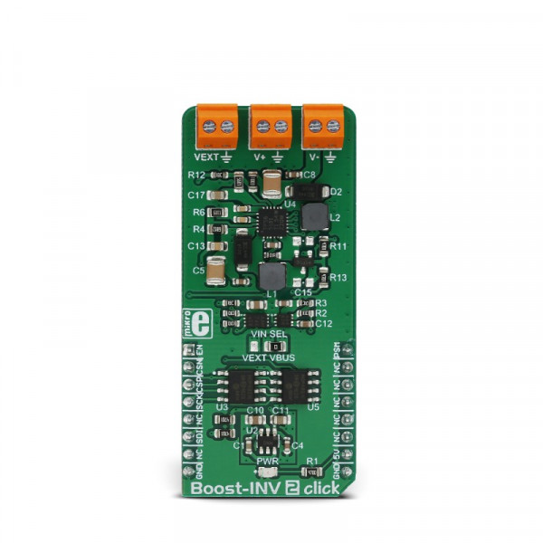
Boost-INV 2 click


- Order number: MIKROE-3123
Advanced switching control of the TPS65131 with a self-learning feedback correction characteristic allows high efficiency and less dissipation. Low output voltage ripple reduces EMI, allowing the converter to be used for sensitive applications. Soft start feature prevents startup inrush current, while the output disconnect feature prevents current leaking (battery discharge) when the device is powered off. These features allow this Click board™ to be used as a very compact programmable split-rail power supply used for general purpose applications, low power audio applications, LCD and OLED displays and similar applications that use dual power supply source.
How does it work?
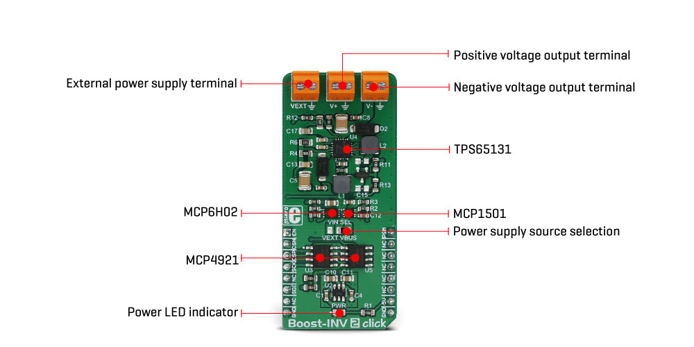
Boost-INV 2 click features a set of integrated circuits which are used to achieve digitally controlled output voltage. The main converter IC is the TPS65131, a positive and negative output DC/DC Converter, from Texas Instruments. Two D/A converters are connected into the positive and negative voltage feedback loop of the TPS65131. The positive and the negative loops are fed into the internal error amplifiers, which compare the feedback voltage with the internal references. They change the duty cycle of the output switching sections in order to compensate for the differences (errors), affecting the output voltage that way. Incorporating a D/A converter into the feedback loop allows programmed "errors" to be introduced into the loop, which in return allows control over the output voltage.
The TPS65131 IC uses the fixed frequency PWM signal to switch its output stages. The internal current limitation is set to about 1950 mA for both the inverting and boost converter. While running in the continuous conduction mode, the output voltage is clean, with no significant ripple and noise. The complete disconnect of both inverting and boosting converter stages allows no source current flowing through the converter, while it is unpowered. This prevents battery draining, making the device able to use the battery power, providing a split-rail power supply for various applications.
Two D/A converters (DAC) labeled as MCP4291, 12-Bit DACs with the SPI Interface by Microchip, are used in feedback loops. One of the DACs is connected to the MCP6H02 op-amp, configured as the inverting unity gain amplifier. It inverts the polarity of the DAC signal. The feedback voltage of the inverting converter can vary from 0V (Vref) to -15V. Therefore, the DAC signal which commonly ranges from 0 to +VREF, needs to be inverted. For the boost converter, there is no need to invert the DAC, so its voltage goes up to +VREF. There are two separate CS pins (Chip Select) for these DACs, so both can be programmed independently. Those Chip Select pins are routed to the RST and CS pins of the mikroBUS™ and are labeled as CSN for the negative voltage controlling DAC, and CSP for the positive voltage controlling DAC.
Two more auxiliary ICs are used on the Boost-INV 2 click. One IC is the ADM8829, a switched-capacitor voltage inverter which provides a negative supply voltage for the inverting op-amp. The other IC is the MCP1501, a high precision buffered voltage reference required for the DACs (4.096 V).
The TPS65131 converter IC can be operated in the Power Saving mode. This is very useful for low currents because the device will power itself down as long as the voltage across the output stays above the internally set threshold. When the voltage drops under this threshold, the converter powers up and produces several switching pulses recovering the nominal voltage value across the load, and powers down again. Depending on the connected load, it will take more or less time to drain the charge from the inductor. Unlike the normal mode, which operates in the continuous-conduction mode (CCM), power saving mode allows the converter to switch between CCM and DCM (discontinuous-conduction) modes. The Click board™ has its PWM pin routed to the PSP and PSN pins of the TPS65131 IC, and HIGH logic level on this pin will put the IC into the Power Saving mode. The PWM pin of the mikroBUS™ is labeled as the PSM on this Click board™.
When the ENP and ENN pins of the TPS65131 IC are at the LOW logic level, the device is completely powered down, disconnecting the loads as described above, preventing current leakage through the passive elements of the circuit. These pins are routed to the AN pin of the mikroBUS™ and labeled as EN, allowing the host MCU to control the operation of the Click board™
By default, the input voltage is taken from the mikroBUS™ +5V power rail. An onboard VIN SEL jumper allows selection between the +5V from the mikroBUS™ or an external power supply connected to the screw terminal input, which is labeled as VEXT. The remaining two screw terminals are negative and positive voltage outputs, labeled as V- and V+. All three screw terminals share a common GND.
Specifications
| Type | Boost |
| Applications | The Click board™ can be used as a very compact programmable split-rail power supply used for general purpose applications, low power audio applications, LCD and OLED displays and similar applications that use dual power supply source |
| On-board modules | TPS65131, a positive and negative output DC/DC converter by Texas Instruments; MCP4291, a 12-Bit DACs; MCP6H02, a dual operational amplifier, MCP1501, a high precision buffered voltage reference, all by Microchip; ADM8829, a switched-capacitor voltage inverter by Analog Devices |
| Key Features | Programmable output positive and negative voltage up to ±15V from a single-sided low voltage, reasonably high current output, high efficiency, soft start, complete load disconnect when powered off, and more |
| Interface | GPIO,SPI |
| Input Voltage | 5V |
| Click board size | L (57.15 x 25.4 mm) |
Pinout diagram
This table shows how the pinout on Boost-INV 2 click corresponds to the pinout on the mikroBUS™ socket (the latter shown in the two middle columns).
| Notes | Pin | Pin | Notes | ||||
|---|---|---|---|---|---|---|---|
| Chip Enable | EN | 1 | AN | PWM | 16 | PSM | Power Save Mode |
| Chip Select (Negative) | CSN | 2 | RST | INT | 15 | NC | Ready |
| Chip Select (Negative) | CSP | 3 | CS | RX | 14 | NC | |
| SPI Clock | SCK | 4 | SCK | TX | 13 | NC | |
| NC | 5 | MISO | SCL | 12 | NC | ||
| SPI Data-In | SDI | 6 | MOSI | SDA | 11 | NC | |
| NC | 7 | 3.3V | 5V | 10 | 5V | Power supply | |
| Ground | GND | 8 | GND | GND | 9 | GND | Ground |
Onboard Jumpers and Settings
| Label | Name | Default | Description |
|---|---|---|---|
| LD1 | PWR | - | Power LED indicator |
| JP1 | VIN SEL | Right | Input voltage selection: left position - external power supply, right position - 5V from mikroBUS |
| JP2 | I2C ADD | Right | I2C address selection: left position 0x49h, right position 0x69h |
| TB1 | GND, V+ | - | Positive voltage output terminal |
| TB2 | GND, V- | - | Negative voltage output terminal |
| TB3 | GND, VEXT | - | External programming voltage header |
Boost-INV 2 click electrical specifications
| Description | Min | Typ | Max | Unit |
|---|---|---|---|---|
| Input voltage (VIN) | 2.7 | 5 | 5.5 | V |
| Positive output voltage (boost converter) | VIN+0.5 | - | 15 | V |
| Negative output voltage (inverting converter) | -2 | - | -15 | V |
| Switching current limit on V+ (boost converter) | 1700 | 1950 | 2200 | mA |
| Switching current limit on V- (inverting converter) | 1700 | 1950 | 2250 | mA |
Software support
We provide a demo application for Boost-INV 2 click on our Libstock page, as well as a demo application (example), developed using MikroElektronika compilers. The demo can run on all the main MikroElektronika development boards.
Library Description
The library initializes and defines SPI drivers along with the driver that gives an option to set desired positive and negative output voltages.
Key functions:
void boostinv2_enable()- Functions for enable chip.void boostinv2_setPositiveVoltage( uint16_t voltage )- Functions for set positive output voltage.void boostinv2_setNegativeVoltage( uint16_t voltage )- Functions for set negative output voltage.
Example description
The application is composed of three sections:
- System Initialization - Initializes the I2C module and sets RST, AN, CS and PWM pin as OUTPUT
- Application Initialization - Initializes Driver init and enable chip
- Application Task - (code snippet) - Changes the positive and negative output voltage. Positive output voltage goes from 5V to 15V with Negative output voltage goes from -5V to -15V
void applicationTask()
{
/* Positive output voltage */
boostinv2_setPositiveVoltage( _BOOSTINV2_POS_VOUT_6V );
Delay_ms( 3000 );
boostinv2_setPositiveVoltage( _BOOSTINV2_POS_VOUT_8V );
Delay_ms( 3000 );
boostinv2_setPositiveVoltage( _BOOSTINV2_POS_VOUT_12V );
Delay_ms( 3000 );
boostinv2_setPositiveVoltage( _BOOSTINV2_POS_VOUT_14V );
Delay_ms( 3000 );
boostinv2_setPositiveVoltage( _BOOSTINV2_POS_VOUT_12V );
Delay_ms( 3000 );
boostinv2_setPositiveVoltage( _BOOSTINV2_POS_VOUT_8V );
/* Negative output voltage */
boostinv2_setNegativeVoltage( _BOOSTINV2_NEG_VOUT_5V );
Delay_ms( 3000 );
boostinv2_setNegativeVoltage( _BOOSTINV2_NEG_VOUT_7V );
Delay_ms( 3000 );
boostinv2_setNegativeVoltage( _BOOSTINV2_NEG_VOUT_13V );
Delay_ms( 3000 );
boostinv2_setNegativeVoltage( _BOOSTINV2_NEG_VOUT_7V );
}
The full application code, and ready to use projects can be found on our Libstock page.
Other MikroElektronika libraries used in the example:
- SPI
Additional notes and information
Depending on the development board you are using, you may need USB UART click, USB UART 2 click or RS232 click to connect to your PC, for development systems with no UART to USB interface available on the board. The terminal available in all MikroElektronika compilers, or any other terminal application of your choice, can be used to read the message.
mikroSDK
This click board is supported with mikroSDK - MikroElektronika Software Development Kit. To ensure proper operation of mikroSDK compliant click board demo applications, mikroSDK should be downloaded from the LibStock and installed for the compiler you are using.
For more information about mikroSDK, visit the official page.
Downloads
mikroBUS™ Standard specificationBoost-INV 2 click: 2D and 3D files