
Nano Power click


- Order number: MIKROE-3035
- Manufacturer product ID: MIKROE-3035
Nano Power click is a boost (step-up) DC-DC converter click with extremely high efficiency and very low input voltage, aimed at the low power IoT market and battery-powered sensors and other devices. The input voltage can be very low: the conversion will start for voltages down to 0.95V, providing 5V to the connected load. Once started, the input voltage can drop as low as the 0.4V, depending on the connected load. The onboard DC-DC converter IC uses the pulse frequency modulation control scheme (PFM), that allows high efficiency and low power consumption for a wide range of output currents.
The DC-DC boost IC requires a minimum number of components. It features True Disconnect™ proprietary technology which completely separates the input and the output stages. It also features the Enable (EN) pin transient protection feature (ETP), which protects the EN pin of transients influence, providing a regulated output voltage. These features make the Nanopower click an ideal solution for low power applications, such as the battery-powered IoT applications, low power wireless devices, battery operated wearable sensors and devices, supercapacitor backup power applications (e.g. UPS click), and other applications that require absolutely low power and high-efficiency DC-DC step-up voltage conversion.
How does it work?
This Click board™ is aimed towards very low power consumption from the connected power supply, while providing stabilized 5V on the output. This is possible only by using a very efficient DC-DC converter, such as the MAX17222 - a nanoPower synchronous boost converter with True Shutdown™ technology, from Maxim Integrated. The device operates in several different modes, which allow optimal utilization of the available power. The device will automatically switch to a different working mode depending on the connected load, providing optimal conditions for a given situation. The MAX17222 uses the pulse frequency modulation control (PFM) topology, which allows high efficiency over a wide range of output currents. The PFM control allows both continuous and discontinuous (CCM and DCM) switching modes to be used.
 Operation of the MAX17222 changes with the connected load, as mentioned above. When the load is very light, the device operates in the Ultra Low Power Mode (ULPM) and the switching is performed in discontinuous mode (DCM). The ULPM is typically used when the device connected at the output is in standby or power down mode, draining a very low amount of current. As the current requirement increases, the MAX17222 device switches to the Low Power mode and further to the High Power mode (LPM and HPM). These modes result in cleaner output and less ripple than the ULPM mode. When working in HPM, the continuous switching mode (CCM) is used (with no pulses being skipped), providing low noise, ripple free output voltage, which is suitable for various sensor measurements, A/D conversions, wireless communication, and other noise and ripple sensitive applications.
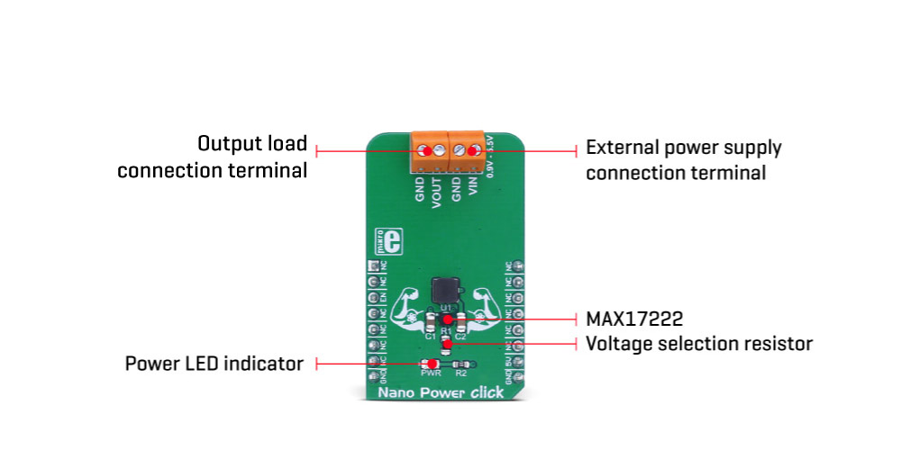
The EN pin of the MAX17222 is used to enable this device. When a transition from LOW to HIGH logic state appears at this pin (rising edge), it will activate the IC and regulated 5V will appear at the output (providing that the proper input voltage is present). This pin is routed to the mikroBUS™ CS pin, which is labeled as EN. The device will remain enabled, even if the input voltage drops to 0.4V, thanks to the internal ETP section of the MAX17222 IC. Holding the EN pin to a HIGH logic state once the conversion is started results in slightly increased power consumption.
The Power LED indicator is connected to the 5V rail of the mikroBUS™ and does not affect the power consumption on the connected external power supply. The power consumption calculations that can be found in the datasheet, remain true and not affected by any external components of this Click board™. The Power LED indicates the presence of the mikroBUS™ voltage, signaling that the EN pin can be controlled via the host MCU.
The external power supply can be connected to the input terminals, between the VIN and GND, ranging from 0.95V up to 5.5V. However, for an optimal operation of the Nanopower click, the input voltage should be lower than the output voltage. The Nanopower click allows maximum peak current of 500mA before the current limit protection activates.
The output voltage is fixed at 5V by a single resistor, connected between the SEL pin of the IC and GND. This resistor is 0 ? and it is basically - an SMD jumper. By using other values (listed in the datasheet of the MAX17222 IC) it is possible to change the output voltage to a value different than 5V. Please consult the datasheet for a proper selection of the resistor for the given output voltage.
The control of the Nanopower click is extremely simple and it is reduced to controlling a single pin. However, provided library offers functions that simplify and speed up the application development even more. The included example application demonstrates their use. This application can be used as a reference for custom projects.
Specifications
| Type | Boost |
| Applications | Ideal solution for low power applications, such as the battery-powered IoT applications, low power wireless devices, battery operated wearable sensors and devices, supercapacitor backup power applications (e.g. UPS click), etc. |
| On-board modules | MAX17222, 400mV to 5.5V Input, nanoPower synchronous boost converter with True Shutdown™ technology |
| Key Features | High efficiency with True Disconnect technology, very low power consumption, very low input voltage operational requirements, low count of components, ETP for the EN pin, efficient PFM switching. |
| Interface | GPIO |
| Input Voltage | 5V |
| Click board size | M (42.9 x 25.4 mm) |
Pinout diagram
This table shows how the pinout on Nano Power click corresponds to the pinout on the mikroBUS™ socket (the latter shown in the two middle columns).
| Notes | Pin | Pin | Notes | ||||
|---|---|---|---|---|---|---|---|
| NC | 1 | AN | PWM | 16 | NC | ||
| NC | 2 | RST | INT | 15 | NC | ||
| Chip Enable IN | EN | 3 | CS | RX | 14 | NC | |
| NC | 4 | SCK | TX | 13 | NC | ||
| NC | 5 | MISO | SCL | 12 | NC | ||
| NC | 6 | MOSI | SDA | 11 | NC | ||
| NC | 7 | 3.3V | 5V | 10 | +5V | Power supply | |
| Ground | GND | 8 | GND | GND | 9 | GND | Ground |
Nano Power click electrical specifications
| Description | Min | Typ | Max | Unit |
|---|---|---|---|---|
| Peak current limit | 400 | 500 | 575 | mA |
| Input voltage range (for normal operation) | 0.95 | - | 5.5 | V |
| External power supply connection terminal | - | 5.0 | - | V |
Onboard settings and indicators
| Label | Name | Default | Description |
|---|---|---|---|
| LD1 | PWR | - | Power LED indicator |
| TB1 | VOUT GND | - | Output load connection terminal |
| TB2 | VIN GND | - | External power supply connection terminal |
Software support
We provide a demo application for Nano Power click on our Libstock page, as well as a demo application (example), developed using MikroElektronika compilers. The demo can run on all the main MikroElektronika development boards.
Library Description
Library initializes and defines GPIO driver and performs control of device voltage.
For more details check the documentation.
Key functions:
void nanopw_enableDevice( const uint8_t state )- The function allows or blocks the input voltage (enables or disables device).
Example description
The application is composed of three sections:
- System Initialization - Initializes ENABLE (RST) pin as an output.
- Application Initialization - Initializes the GPIO driver.
- Application Task - (code snippet) - Turns the device on for 5 seconds and then turns the device off for 10 seconds. Afterward, the output voltage starts to fall.
When the input voltage rises from 0.8V to 5.5V, the output voltage rises from 5.1V to 5.25V. When the input voltage is less than 0.8V, the output voltage is less than 5V.
void applicationTask()
{
nanopw_enableDevice( _NANOPW_ENABLE_DEVICE );
Delay_ms( 5000 );
nanopw_enableDevice( _NANOPW_DISABLE_DEVICE );
Delay_ms( 10000 );
}
The full application code, and ready to use projects can be found on our Libstock page.
Additional notes and information
Depending on the development board you are using, you may need USB UART click, USB UART 2 click or RS232 click to connect to your PC, for development systems with no UART to USB interface available on the board. The terminal available in all MikroElektronika compilers, or any other terminal application of your choice, can be used to read the message.
mikroSDK
This click board is supported by mikroSDK - MikroElektronika Software Development Kit. To ensure proper operation of mikroSDK compliant click board demo applications, mikroSDK should be downloaded from the LibStock and installed for the compiler you are using.