
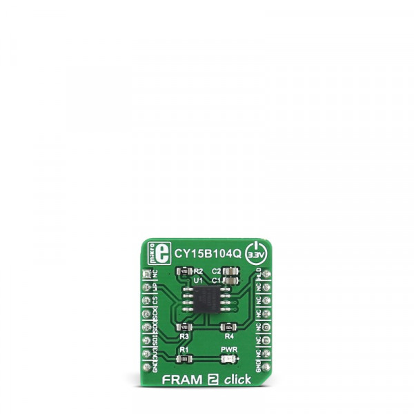
FRAM 2 click


- Order number: MIKROE-2768
- Manufacturer product ID: MIKROE-2768
FRAM 2 click carries the CY15B104Q 4-Mbit (512K x 8) serial F-RAM. A ferroelectric random-access memory or F-RAM is non-volatile and performs reads and writes similar to a SRAM. You can access the memory using an industry-standard serial peripheral interface (SPI) bus.
On the functional level, the F-RAM operates in a similar way as serial flash and serial EEPROMs. The major difference between the CY15B104Q and a serial flash or EEPROM with the same pinout is the F-RAM's superior write performance, high endurance, and low power consumption.
CY15B104Q FRAM features
Low power consumption, high endurance and 4-Mbit of non-volatile memory - these are some of the many reasons you'll want to use this in your work.
The CY15B104Q is ideal for non-volatile memory applications, requiring frequent or rapid writes. Examples range from data collection, where the number of write cycles may be critical, to demanding industrial controls where the long write time of serial flash or EEPROM can cause data loss.
.jpg)
Unlike serial flash and EEPROM, the CY15B104Q performs write operations at bus speed. No write delays are incurred. Data is written to the memory array immediately after each byte is successfully transferred to the device.
The CY15B104Q is capable of supporting 10^14 read/write cycles, or 100 million times more write cycles than EEPROM.
How the click works
When accessing the CY15B104Q, the user addresses 512K locations, each containing eight data bits. These eight data bits are shifted in or out serially. The addresses are accessed using the SPI protocol.
Cypress's CY15B104Q is an SPI slave device and operates at speeds up to 40 MHz. This high-speed serial bus provides high-performance serial communication to an SPI master. SPI pins of an IC are connected to SPI pins of mikroBUS™ so it can be driven by a microcontroller on one of our various development systems - clicker and clicker 2 development boards, Flip&Click boards, click shields, our famous EasyPIC v7 and more.
The HLD (HOLD_N) pin can be used to interrupt a serial operation without aborting it. The WP (WP_N) pin ensures hardware write protect feature if the write protect enable bit in the Status Register is set to ’1’. The SPI protocol includes a chip select (to permit multiple devices on the bus), an opcode, and a three-byte address. There are nine opcodes, that can be issued by the bus master to the CY15B104Q. These opcodes specify the commands from the bus master to the slave device. After the CS (CS_N) is activated, the first byte transferred from the bus master is the opcode. Following the opcode, any addresses and data are then transferred. The CS (CS_N) must go inactive after an operation is complete and before a new opcode can be issued.
click boards are plug and play!
Up to now, MikroElektronika has released hundreds of click boards™. We are releasing new ones every week. It is our intention to provide you with as many add-on boards as possible, so you will be able to expand your development board with additional functionality.
Pull-up resistors are included on the FRAM 2 click and it's ready to be used immediately after plugging into the mikroBUS™ socket on one of our development boards.
Ferroelectric RAM
Ferroelectric RAM, better known as FRAM is a random-access memory. It's famous for fast access times and low power consumption. Also, since it's a non-volatile type of memory, data is retained upon power down.
This type of memory is used in many industries today, but most commonly in small hand-held devices, since it has low power consumption, like mobile phones, electronic meters, medical applications, etc.
Specifications
| Type | FRAM |
| Applications | Suitable for low-power applications |
| On-board modules | CY15B104Q - a 4-Mbit non-volatile memory employing an advanced ferroelectric process |
| Key Features | 4-Mbit ferroelectric random access memory (F-RAM) logically organized as 512 K × 8, high-endurance 100 trillion (10^14) read/writes, 151-year data retention, low power consumption |
| Interface | GPIO,SPI |
| Input Voltage | 3.3V |
Pinout diagram
This table shows how the pinout on FRAM 2 click corresponds to the pinout on the mikroBUS™ socket (the latter shown in the two middle columns).
| Notes | Pin | Pin | Notes | ||||
|---|---|---|---|---|---|---|---|
| NC | 1 | AN | PWM | 16 | HLD | Hold | |
| Write protect | WP | 2 | RST | INT | 15 | NC | |
| Chip select | CS | 3 | CS | TX | 14 | NC | |
| SPI clock pin | SCK | 4 | SCK | RX | 13 | NC | |
| SPI slave data out pin | SDO | 5 | MISO | SCL | 12 | NC | |
| SPI slave data in pin | SDI | 6 | MOSI | SDA | 11 | NC | |
| Power supply | +3.3V | 7 | 3.3V | 5V | 10 | NC | |
| Ground | GND | 8 | GND | GND | 9 | GND | Ground |
Programming
Code examples for FRAM 2 click, written for MikroElektronika hardware and compilers are available on Libstock.
Code snippet
This code snippet shows one part of the example provided alongside with the click board™. The task writes value 42 into the memory address 0x10 and then the read value from the same memory part. The read value should match the written value (42).
01 void Fram_2_Task()
02 {
03     uint8_t readData;
04     char outputText [5];
05     memset ( outputText, 0, 5);
06     UART1_Write_Text ("rnWriting value 42 into register 0x10...");
07     Fram_2_Write (0x00, 0x00, 0x10, 42 );
08
09     UART1_Write_Text ("rnReading from register 0x10...");
10     readData = Fram_2_Read  (0x00, 0x00, 0x10);
11     ShortToStr (readData, outputText);
12     UART1_Write_Text ("rnRead value: ");
13     UART1_Write_Text (outputText);
14 }